Nonfilamentary Switching with Trap-Controlled Capacitive Charge Modulation in GaOx/HfOx Heterostructures on Flexible Substrate
IEEE Transactions on Electron Devices (2026)
DOI: https://doi.org/10.1109/TED.2026.3708423
Below are the list of some recent publications, organized by their types. Each section is further arranged in a chronological order (newest first).
IEEE Transactions on Electron Devices (2026)
DOI: https://doi.org/10.1109/TED.2026.3708423
Physica Scripta, 101, 275102 (2026)
DOI: https://doi.org/10.1088/1402-4896/ae82ce
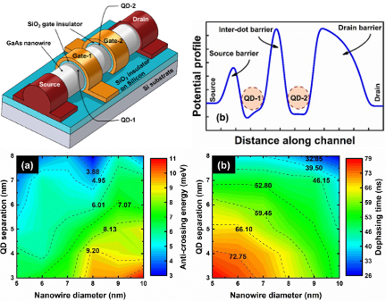
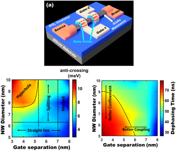
Quantum bits (qubits) realized by generating quantum dots (QDs) in state-of-the-art nanoscale field-effect transistors (FETs) are promising candidates for scalable quantum information processing systems. However, the transport properties of QDs in FET architectures, and hence the device performance, depend significantly on the size and position of QDs placed along the channel. In this context, current work studies the impact of geometrical design parameter engineering on the transport properties of double quantum dots (DQDs) realized in nanowire FET architectures for possible charge qubit generation. Using non-equilibrium Green’s function formalism, the effects of QD size and their separation on the transport diagrams, inter-dot coupling strength and drain tunneling-dependent escape lifetime are studied by varying the nanowire diameter and inter-gate separation. The study suggests that increased nanowire diameter enhances inter-dot coupling but at the cost of reduced escape lifetime. On the other hand, increasing the inter-gate separation degrades both inter-dot coupling and escape lifetime. Consequently, a design window is suggested for relatively high inter-dot coupling strength in the ~8–11 meV range and escape lifetimes in the ~50–75 ns range. The performance parameters exhibit a strong dependence on the channel effective mass but insignificant dependence on permittivity, suggesting the possibility of further tuning the device performance in such architectures.
Journal of Materials Science: Materials in Electronics, 36, 2304 (2025)
DOI: https://doi.org/10.1007/s10854-025-16334-1
In this article, highly conductive p-type Ga-doped ZnO (GZO) films are thermally grown by engineering the oxygen interstitial (Oi) and zinc vacancy (VZn)-related intrinsic acceptor-type defects. Ga-doping controlled defect engineering approach in GZO films has been adopted for optimizing its optical transparency and electrical conductivity. The effects of Ga doping (0%, 2.5%, 5% and 7.5%) on the structural, morphological, compositional and optical properties of the films are systematically investigated by employing X-ray diffraction (XRD), Scanning electron microscopy (SEM), X-ray photoelectron spectroscopy (XPS) and UV–Vis spectroscopy, respectively. Density functional theory (DFT)-calculations reveal Ga doping to significantly reduce the formation energies of oxygen interstitials and zinc vacancies. Electrical measurements confirm p-type conductivity in all of the doped samples. The 5% Ga-doped ZnO film provides the highest conductivity and figure of merit (F.O.M), and thus, suggesting it to be a promising p-type Transparent Conducting Oxide (TCO) for the future transparent electronic and optoelectronic applications.
Solid-State Electronics, 230, p. 109259 (2025)
DOI: https://doi.org/10.1016/j.sse.2025.109259
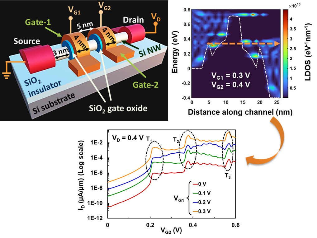
The article deals with the modeling of gate voltage controlled resonant tunneling transport in a complementary-metal–oxide–semiconductor (CMOS) compatible double quantum dot channel nanowire field-effect-transistor (FET). Appropriate applied voltages at two separate gates, gate-1 and gate-2 of the device form two voltage-tunable quantum dots underneath the gates, within the nanowire channel. The quantum dot eigenstates are tuned by varying the applied gate voltages to enable voltage-modulated resonant tunneling transport. Such transport is modeled by employing a Schrödinger-Poisson self-consistent framework using non-equilibrium Green’s function (NEGF) formalism. Electron–phonon scattering within the nanowire channel is also considered. The transfer characteristics exhibit multiple current thresholds in the range of 10^(−4) uA/um – 1 uA/um due to resonant tunneling. The phonon scattering is observed to significantly depend on nanowire geometry and applied gate voltages, with tunneling dominated quasi-ballistic transport occurring at higher gate voltages. Also, steep sub-threshold slopes of 30 mV/decade–8 mV/decade range and transconductance in the range of 10^(−7) uS/um – 1 uS/um at room temperature are obtained by varying the nanowire diameter in the range of 20 nm – 5 nm. Therefore, such device architecture exhibits significant potential for achieving multi-current thresholds in a CMOS compatible architecture at room temperature.
Journal of Electronic Materials, 54, pp. 9511 - 9523 (2025)
DOI: https://doi.org/10.1007/s11664-025-12059-3
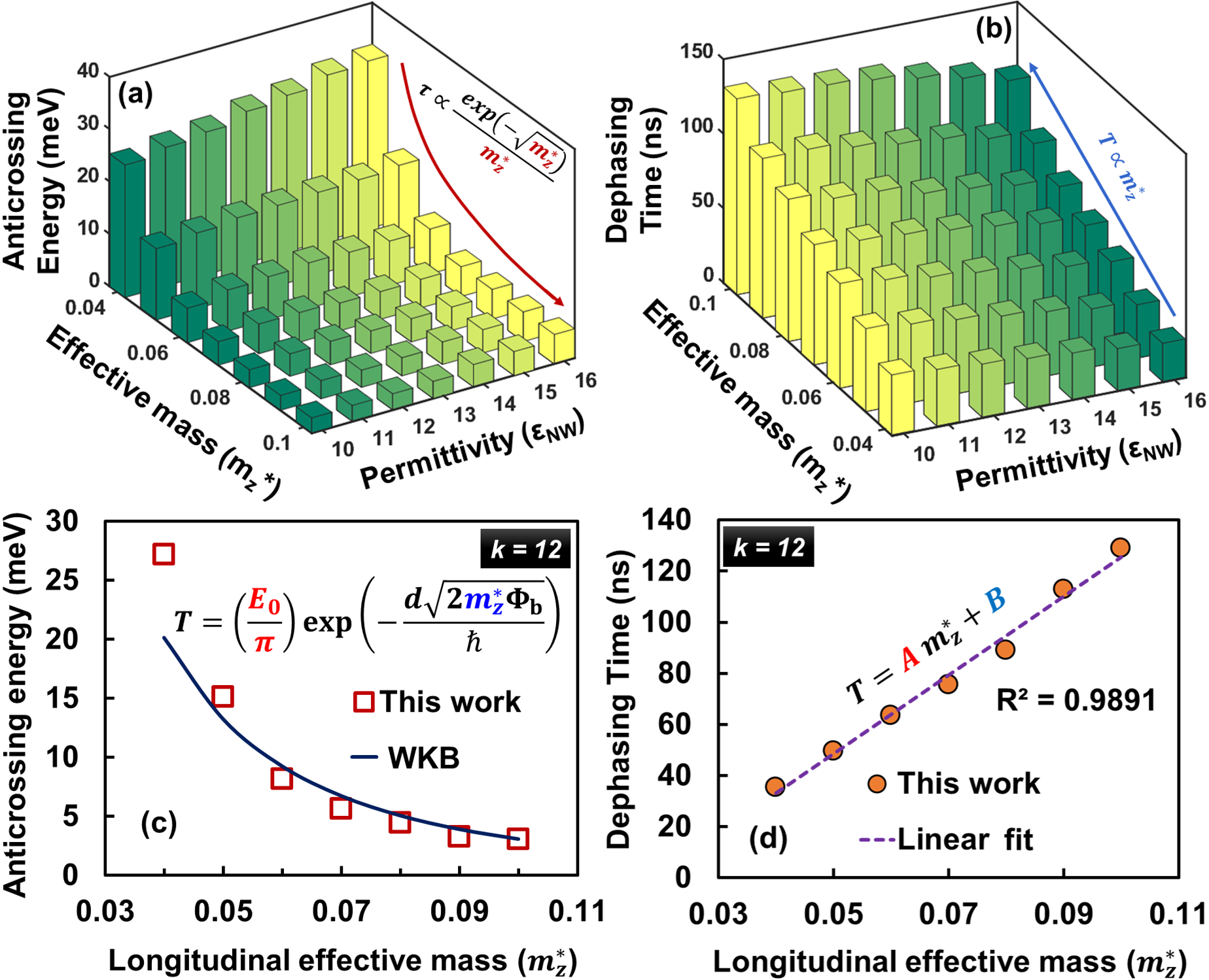
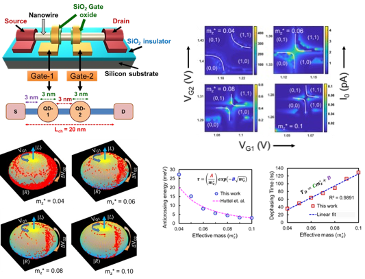
This work investigates the material-dependent charge qubit performance of a gate voltage-induced double-quantum-dot gate nanowire channel field-effect transistor (DQD-NWFET) device through charge stability, Bloch sphere coverage, anti-crossing energy, and dephasing time. In this device, voltages at two localized gates along the nanowire channel create two quantum dots in series, which are further tuned by these voltages for the relevant qubit operations. To understand the material-dependent performance of the device, a self-consistent Schrodinger-Poisson framework coupled to non-equilibrium Green’s function formalism is developed. The study indicates that the charge qubit performance of the device significantly depends on the transport effective mass, with slight dependence on nanowire permittivity. It is observed that the increase in transport effective mass leads to sharpening of the “hyperbolic” nature of the charge stability diagram, along with a significant reduction in anti-crossing energy and Bloch sphere coverage. Consequently, anti-crossing energy in the range of 3–25 meV and dephasing time in the range of 25–130 ns can be achieved by varying the transport effective mass and nanowire permittivity from 0.04 to 0.10 and 10–16, respectively. The performance of the device is further studied for specific nanowire materials by taking into account the appropriate material parameters. Therefore, this study enables material engineering of nanowire FET devices for realizing superior charge qubit performance.
(Accepted) IEEE Computer Society Annual Symposium on VLSI: ISVLSI 2026
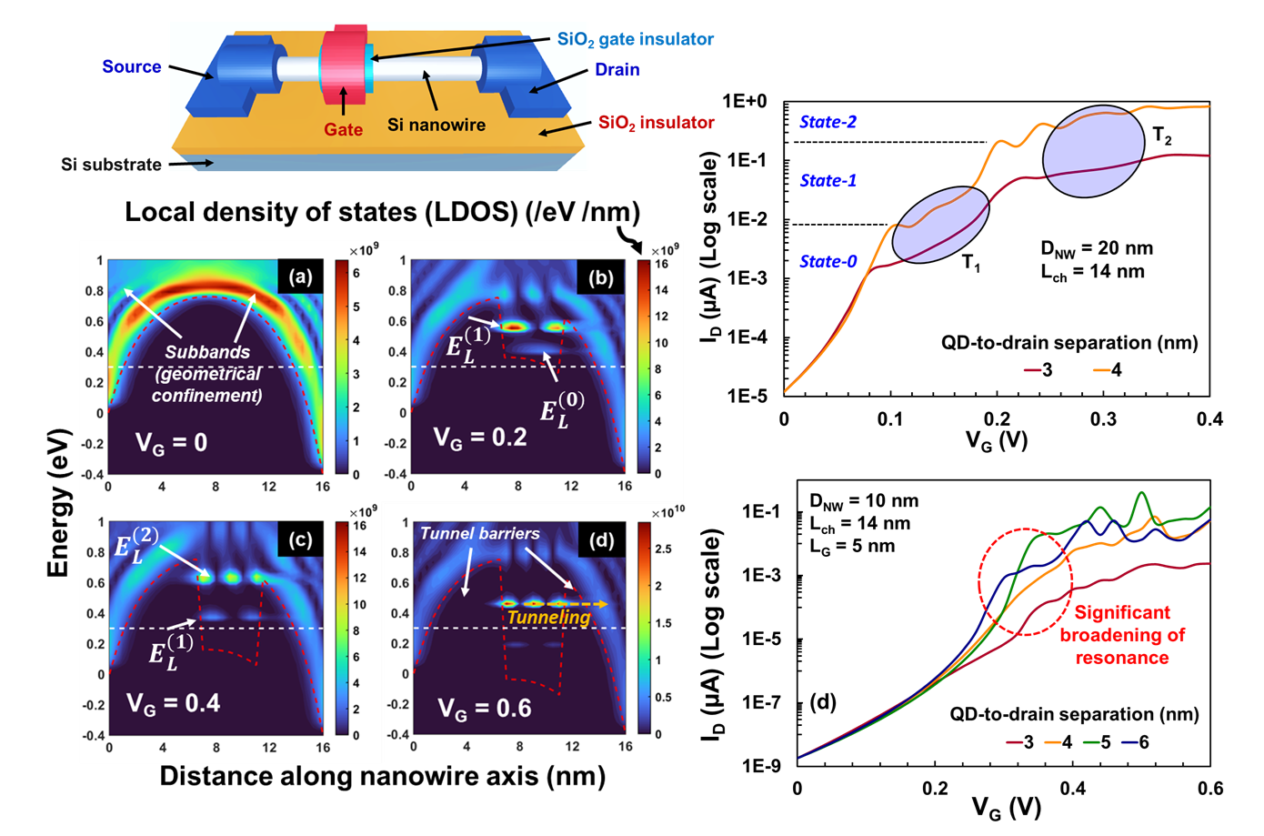
The successive downscaling approach to transistor miniaturization, especially for the binary logic paradigm, faces severe bottlenecks in the present era of 'big data'. Multi-valued logic is being pursued as a potential alternative to alleviate these bottlenecks, with quantum dots (QDs) being envisioned as the key building blocks. Tunneling of electrons through the QD energy states can enable multi-threshold current generation, with potential tunability in terms of QD sizes. Further, QDs hosted in nanoscale field-effect transistors can benefit from the already mature fabrication technologies. Therefore, the current work considers the design of tunnel-engineered double quantum dots realized in silicon nanowire field-effect transistors for multi-threshold current generation. The effects of QD size and position along the channel are studied employing non-equilibrium Green's function formalism. Devices with large nanowire diameters (~20 nm) facilitate multi-threshold current generation. These thresholds are highly susceptible to QD-2 position along the channel, exhibiting sub-thermal sub-threshold swings in the 12 -- 46 mV/decade range. The model is further extended to incorporate localized 'spreading' of gate voltages in view of the practical realization. Upto 5 achievable thresholds and current densities in the ~10^{-4} - ~10^{10} A/m^2 range are observed by tuning the `spreading' of gate potential.
1st International Conference on Sustainable Technologies (ICST), 12th - 14th December, 2024
2nd International Conference on Low Energy Devices (ICLED), 1st - 4th August, 2024
22nd International Workshop on the Physics of Semiconductor Devices, 13th - 17th December, 2023
5th International Symposium on Devices, Circuits and Systems, 2022
DOI: https://doi.org/10.1007/978-981-99-0055-8_20
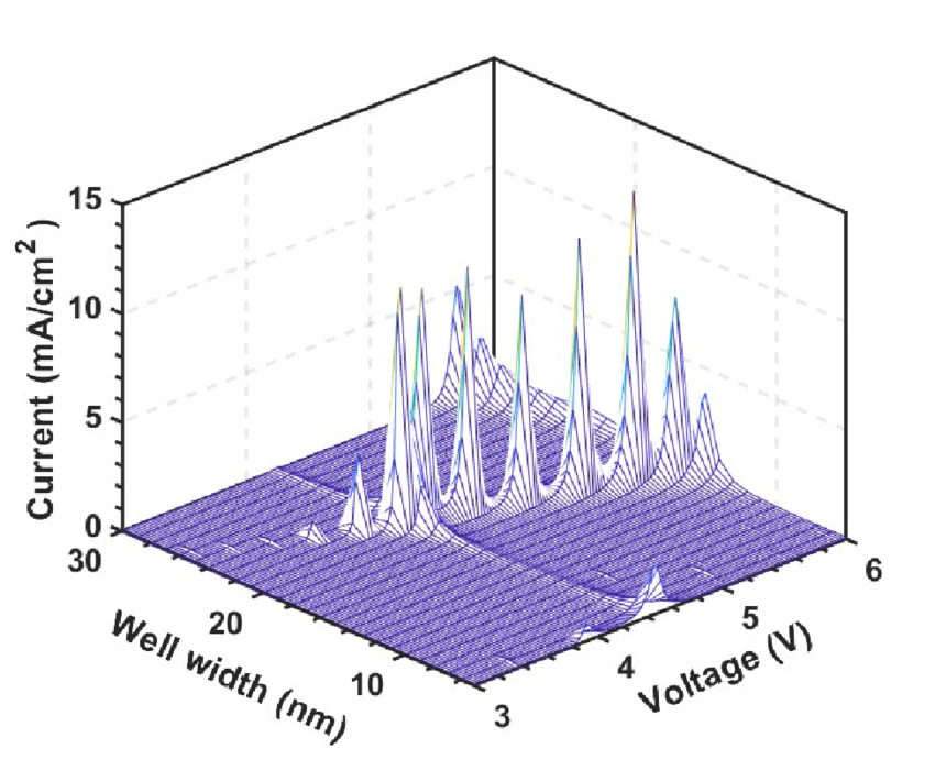
In this work, a Si/SiO2/Ge/SiO2/Pt resonant tunneling device (RTD) with an asymmetric double barrier has been modeled by adopting NEGF formalism. The impact of Ge-quantum well widths below, equal and above its ex-citonic Bohr radius (EBR ~25 nm) on resonant tunneling current is investigated at room temperature. The tunneling current peaks are observed to appear for decreasing the well width to equal or less than the EBR of Ge. Such peak values increase with downscaling of the well width up to a certain value and then it decreases with further miniaturization. The maximum peak current is obtained to be ~13 mA/cm^2 for Ge-well width of 17 nm. The corresponding maximum peak-to-valley current ratio (PVCR) is estimated to be ~18 at room temperature, which is larger in order than the conventional RTDs. Therefore, the current work may provide the route for fabrication of Si/Ge based high performance resonant tunneling devices operational at room temperature.
Preprint (2023)
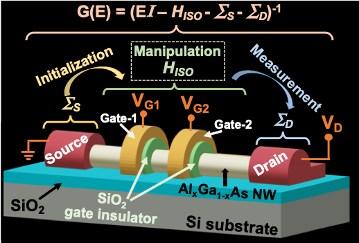
The current work explores a geometrically engineered dual-gate GaAs nanowire FET with stateof-the-art miniaturized dimensions (of nanowire diameter and gate seperation) for high performance charge qubit operation at room temperature. Relevant gate voltages in such device can create two voltage-tunable quantum dots (VTQDs) underneath the gates, as well as can manipulate their eigenstate detuning and the inter-dot coupling to generate superposition, whereas a small drain bias may cause its collapse leading to qubit read-out. Such qubit operations, i.e., ‘Initialization’, ‘Manipulation’, and ‘Measurement’, are theoretically modeled in the present work by developing a second quantization filed operator based Schrodinger-Poisson self-consistent framework coupled to non-equilibrium Green’s function (NEGF) formalism. The study shows that the Bloch sphere coverage can be discretized along polar and azimuthal directions by reducing the nanowire diameter and increasing the inter-dot separation respectively, that can be utilized for selective information encoding. The theoretically obtained stability diagrams suggest that downscaled nanowire diameter and increased gate separation sharpen the ‘bonding’ and ‘anti-bonding’ states with reduced anticrossing leading to a gradual transformation of the ‘hyperbolic’ current mapping into a pair of ‘straight lines’. However, the dephasing time in the proposed GaAs VTQD-based qubit may be significantly improved (~10 ns to ~100 ns) by scaling down both the nanowire diameter and gate separation to ~5-3 nm. Therefore, the present study suggests an optimization window for geometrical engineering of a dual-gate nanowire FET qubit to achieve a selective coverage of Bloch sphere for particular information encoding, stability diagram of desired resolution with minimum anticrossing, and an extensively improved dephasing time. Most importantly, such device is compatible with the mainstream CMOS technology and can be utilized for large scale implementation by little modification of the state-of-the-art fabrication processes.